Alleged AMD Zen 6 Medusa Point APU Surfaces On Geekbench
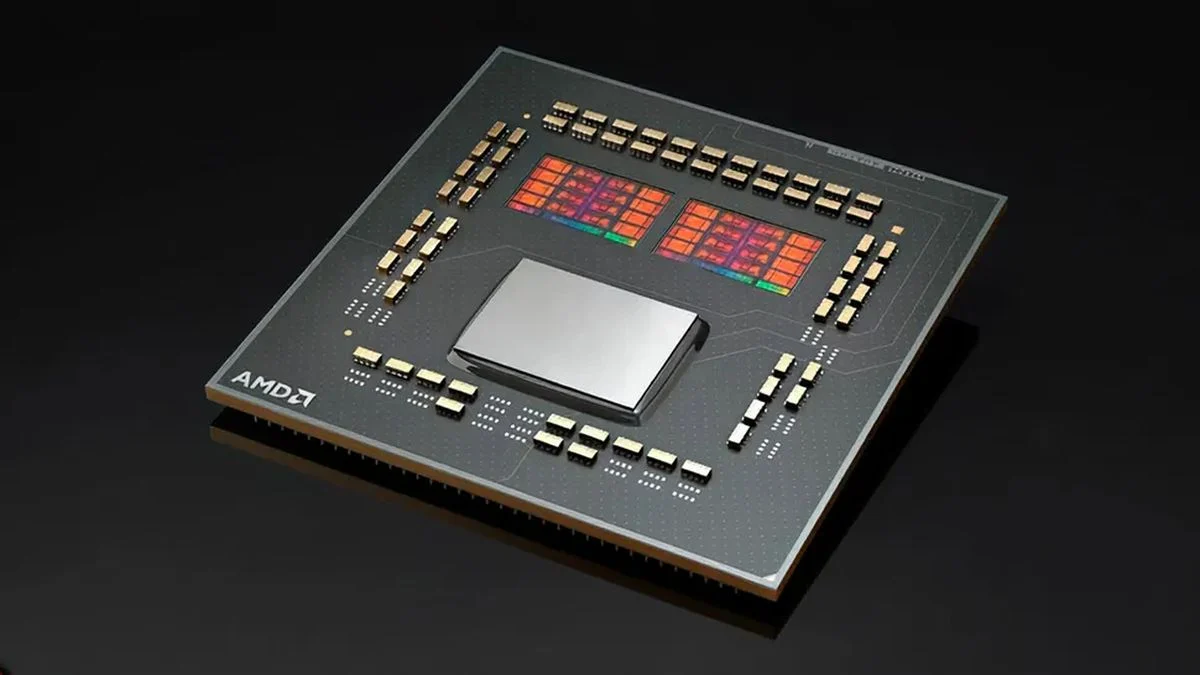
It appears that AMD’s alleged Medusa Point Zen 6 APU has surfaced on Geekbench. Interestingly, the repository shows an interesting core configuration and cluster formation.
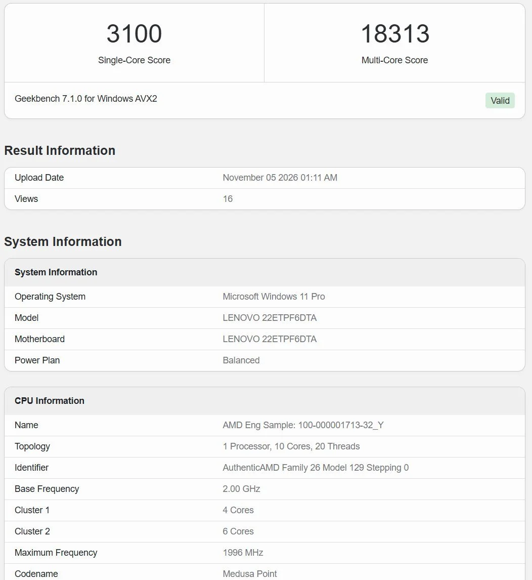
According to the Geekbench listing, the Zen 6 Medusa Point showcases a 10-core, 20-thread configuration for the CPU, and that it is divided into two clusters: four Zen 6 cores and six Zen 6c cores. To explain the difference between the two, think of the Zen 6c cores as the equivalent to Intel’s E-Cores, albeit having a different usage.
Each core is fitted with 32KB of L1 instruction cache, 48KB of L1 data cache, 1MB L2 cache, but a 16MB L3 Cache shared across all 10 cores. Additionally, the repository indicates a 2GHz base clock, but weirdly enough, the boost clock is lower, although this may be a misreading of early silicon, rather than the actual speed.
Further, the instruction set confirms full AVX-512 support, which includes AVX512-FP16 and AVX512-VNNI extensions, and that includes AVX-VNNI. Other details indicate that the Zen 6 Medusa Point APU was tested on a Lenovo-based laptop and paired with 64GB quad-channel DDR5 RAM, running at 5,188MT/s.
AMD’s Zen 6 Medusa Point has been rumoured to be the first mobile processor to introduce Compute Units (CUs) based on the “desktop exclusive” RDNA4 graphics architecture. Specifically, however, those GPU cores will be introduced into a new mobile segment dubbed “RDNA4m”.
More to the point, the alleged Zen 6 Medusa point scored 3,100 point in the single-core test and 18,313 points in the multicore test. By comparison, it beats out the AMD Ryzen AI Max+ 395, which scored 2,742 points in the same single-core test, and 27,412 points in the multicore test.

It has been hinted to us via sources close to us that AMD intends to announce its Zen 6 CPUs at the start of CES 2027. Stay tuned.
(Source: Videocardz, HXL via X, TPU, Geekbench)